- 您现在的位置:买卖IC网 > Sheet目录328 > IDT7054L20G (IDT, Integrated Device Technology Inc)IC SRAM 32KBIT 20NS 108PGA
IDT7054S/L
High-Speed 4K x 8 FourPort? Static RAM
Military, Industrial and Commercial Temperature Ranges
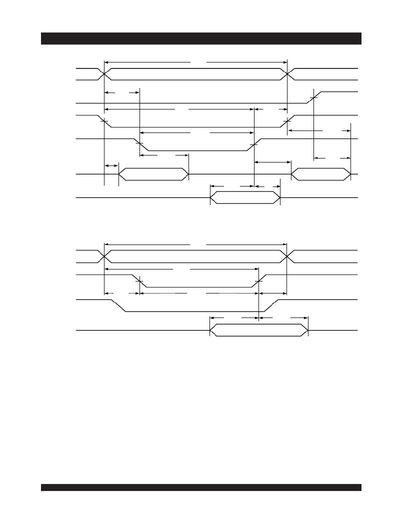
Timing Waveform of Write Cycle No. 1, R/ W Controlled Timing (5,8)
t WC
ADDRESS
t AS
OE
(6)
CE
t AW
t WR
(3)
R/ W
t WP (2)
t HZ
(7)
DATA OUT
t LZ
(4)
t WZ (7)
t OW
(4)
t HZ
(7)
t DW
t DH
DATA IN
3241 drw 07
Timing Waveform of Write Cycle No. 2, CE Controlled Timing (1,5)
t WC
ADDRESS
t AW
CE
t AS
t EW
(6)
(2)
t WR
(3)
R/ W
t DW
t DH
DATA IN
3241 drw 08
NOTES:
1. R/ W or CE = V IH during all address transitions.
2. A write occurs during the overlap (t EW or t WP ) of a CE = V IL and a R/ W = V IL .
3. t WR is measured from the earlier of CE or R/ W = V IH to the end of write cycle.
4. During this period, the I/O pins are in the output state, and input signals must not be applied.
5. If the CE LOW transition occurs simultaneously with or after the R/ W = V IL transition, the outputs remain in the High-impedance state.
6. Timing depends on which enable signal is asserted last, CE or R/ W .
7. Transition is measured 0mV from Low or High-impedance voltage with the Output Test Load (Figure 2). This parameter is guaranteed but is not production tested.
8. If OE = V IL during a R/ W controlled write cycle, the write pulse width must be the larger of t WP or (t WZ + t DW ) to allow the I/O drivers to turn off data to be placed
on the bus for the required t DW . If OE = V IH during an R/ W controlled write cycle, this requirement does not apply and the write pulse can be as short as the
specified t WP .
9
6.42
发布紧急采购,3分钟左右您将得到回复。
相关PDF资料
IDT709089L9PF
IC SRAM 512KBIT 9NS 100TQFP
IDT709099L9PFI
IC SRAM 1MBIT 9NS 100TQFP
IDT709149S10PFI
IC SRAM 36KBIT 10NS 80TQFP
IDT70914S12PF
IC SRAM 36KBIT 12NS 80TQFP
IDT709169L7BFI
IC SRAM 144KBIT 7NS 100FBGA
IDT709279L9PFG
IC SRAM 512KBIT 9NS 100TQFP
IDT709289L9PFI
IC SRAM 1MBIT 9NS 100TQFP
IDT709359L7BFI
IC SRAM 144KBIT 7NS 100FBGA
相关代理商/技术参数
IDT7054L20PRF
功能描述:IC SRAM 32KBIT 20NS 128TQFP RoHS:否 类别:集成电路 (IC) >> 存储器 系列:- 标准包装:3,000 系列:- 格式 - 存储器:EEPROMs - 串行 存储器类型:EEPROM 存储容量:8K (1K x 8) 速度:400kHz 接口:I²C,2 线串口 电源电压:1.7 V ~ 5.5 V 工作温度:-40°C ~ 85°C 封装/外壳:8-SOIC(0.154",3.90mm 宽) 供应商设备封装:8-SOIC 包装:带卷 (TR)
IDT7054L20PRF8
功能描述:IC SRAM 32KBIT 20NS 128TQFP RoHS:否 类别:集成电路 (IC) >> 存储器 系列:- 标准包装:1,000 系列:- 格式 - 存储器:RAM 存储器类型:SRAM - 双端口,同步 存储容量:1.125M(32K x 36) 速度:5ns 接口:并联 电源电压:3.15 V ~ 3.45 V 工作温度:-40°C ~ 85°C 封装/外壳:256-LBGA 供应商设备封装:256-CABGA(17x17) 包装:带卷 (TR) 其它名称:70V3579S5BCI8
IDT7054L25G
功能描述:IC SRAM 32KBIT 25NS 108PGA RoHS:否 类别:集成电路 (IC) >> 存储器 系列:- 标准包装:3,000 系列:- 格式 - 存储器:EEPROMs - 串行 存储器类型:EEPROM 存储容量:8K (1K x 8) 速度:400kHz 接口:I²C,2 线串口 电源电压:1.7 V ~ 5.5 V 工作温度:-40°C ~ 85°C 封装/外壳:8-SOIC(0.154",3.90mm 宽) 供应商设备封装:8-SOIC 包装:带卷 (TR)
IDT7054L25PRF
功能描述:IC SRAM 32KBIT 25NS 128TQFP RoHS:否 类别:集成电路 (IC) >> 存储器 系列:- 标准包装:1,000 系列:- 格式 - 存储器:RAM 存储器类型:SRAM - 双端口,同步 存储容量:1.125M(32K x 36) 速度:5ns 接口:并联 电源电压:3.15 V ~ 3.45 V 工作温度:-40°C ~ 85°C 封装/外壳:256-LBGA 供应商设备封装:256-CABGA(17x17) 包装:带卷 (TR) 其它名称:70V3579S5BCI8
IDT7054L25PRF8
功能描述:IC SRAM 32KBIT 25NS 128TQFP RoHS:否 类别:集成电路 (IC) >> 存储器 系列:- 标准包装:1,000 系列:- 格式 - 存储器:RAM 存储器类型:SRAM - 双端口,同步 存储容量:1.125M(32K x 36) 速度:5ns 接口:并联 电源电压:3.15 V ~ 3.45 V 工作温度:-40°C ~ 85°C 封装/外壳:256-LBGA 供应商设备封装:256-CABGA(17x17) 包装:带卷 (TR) 其它名称:70V3579S5BCI8
IDT7054L25PRFI
功能描述:IC SRAM 32KBIT 25NS 128TQFP RoHS:否 类别:集成电路 (IC) >> 存储器 系列:- 标准包装:3,000 系列:- 格式 - 存储器:EEPROMs - 串行 存储器类型:EEPROM 存储容量:8K (1K x 8) 速度:400kHz 接口:I²C,2 线串口 电源电压:1.7 V ~ 5.5 V 工作温度:-40°C ~ 85°C 封装/外壳:8-SOIC(0.154",3.90mm 宽) 供应商设备封装:8-SOIC 包装:带卷 (TR)
IDT7054L25PRFI8
功能描述:IC SRAM 32KBIT 25NS 128TQFP RoHS:否 类别:集成电路 (IC) >> 存储器 系列:- 标准包装:1,000 系列:- 格式 - 存储器:RAM 存储器类型:SRAM - 双端口,同步 存储容量:1.125M(32K x 36) 速度:5ns 接口:并联 电源电压:3.15 V ~ 3.45 V 工作温度:-40°C ~ 85°C 封装/外壳:256-LBGA 供应商设备封装:256-CABGA(17x17) 包装:带卷 (TR) 其它名称:70V3579S5BCI8
IDT7054L35G
功能描述:IC SRAM 32KBIT 35NS 108PGA RoHS:否 类别:集成电路 (IC) >> 存储器 系列:- 标准包装:3,000 系列:- 格式 - 存储器:EEPROMs - 串行 存储器类型:EEPROM 存储容量:8K (1K x 8) 速度:400kHz 接口:I²C,2 线串口 电源电压:1.7 V ~ 5.5 V 工作温度:-40°C ~ 85°C 封装/外壳:8-SOIC(0.154",3.90mm 宽) 供应商设备封装:8-SOIC 包装:带卷 (TR)
